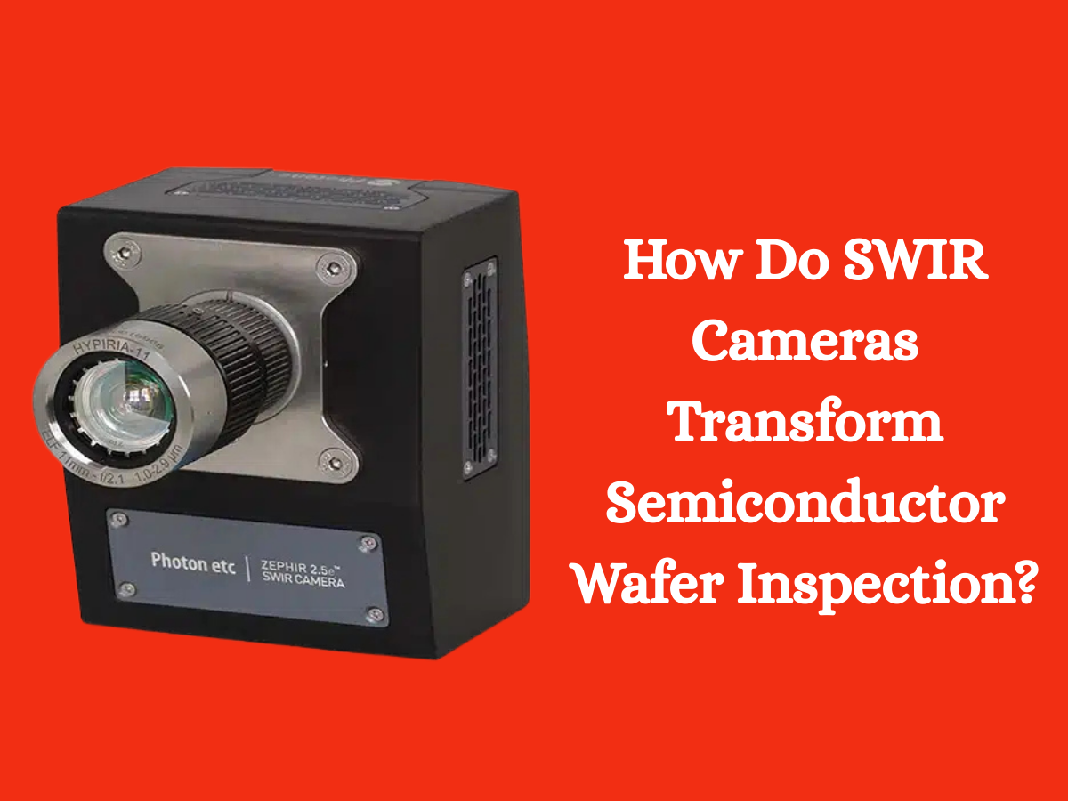
How Do SWIR Cameras Transform Semiconductor Wafer Inspection?
By Pembroke Instruments 23-08-2025 121
Ever wondered what keeps our gadgets running so reliably and uninterrupted, even with continuous usage, with zero to minimal lag? It all starts with the perfect semiconductor wafers, the heart of modern electronics that makes it all possible. A semiconductor wafer is a thin slice of material, usually silicon, used to fabricate integrated circuits and electronic devices, and these are used as substrates to build complex electronic structures like transistors, diodes, etc. Now the SWIR cameras? They are the game-changers that use short-wave infrared light to spot flaws in the semiconductor wafers that regular cameras miss. But how exactly do these cameras revolutionise wafer inspection? Let’s dive into their magic, exploring the ways they’re reshaping the industry with clear, precise answers to our curiosity.
Why Are SWIR Cameras a Must for Wafer Inspection?
What makes SWIR cameras so special? They can see through silicon, unlike visible light cameras. SWIR lights, at wavelengths above 1,000 nm, turn the silicon transparent, revealing hidden cracks, voids, or other impurities inside wafers that are important and vital. Can traditional cameras do this? Nope, they’re blind to subsurface defects. With SWIR cameras, manufacturers catch tiny flaws like micro-cracks or particles, boosting quality and saving more usable chips. And where do they fit in production? Everywhere, from raw silicon ingots to finished wafers. They inspect gently, so no wafer gets damaged. Their sensitivity to certain wavelengths makes them good at spotting the defects. So, why are SWIR cameras essential? They give manufacturers a clear view into wafer quality, ensuring better chips and fewer failures.

How Do SWIR Cameras Work in Semiconductor Inspection?
- Checking Ingots and Semiconductor Wafers
What happens if silicon ingots have flaws? They can damage equipment or ruin wafers later. How do SWIR cameras help? They sneak inside ingots to spot cracks or impurities before slicing. This early catch saves time and resources. For wafers, they reveal subsurface defects like particles or micro-cracks, ensuring only perfect ones move forward. It’s like an X-ray for silicon, keeping production smooth.
- Aligning the Layers and Bonding
How do you stack wafer layers perfectly? SWIR cameras make it possible by imaging through the wafer’s back. Why does this matter? Precise alignment is crucial for building transistors or memory cells. They also check bonding in stacked wafers, catching misalignments or weak spots. So, how do they improve chips? They ensure every layer lines up, making devices faster and more reliable.
- Revealing Failures and Defects
What causes a chip to fail? Tiny cracks or faulty circuits often do. How do SWIR cameras tackle this? They detect glowing emissions from defective circuits, zeroing in on the problem. They also spot micro-cracks or particles that could ruin a chip. Can they handle complex parts? Absolutely, they inspect things like MEMS or optical waveguides, ensuring everything’s solid.
What Makes SWIR Cameras Stand Out Of All?
- Sharp Sensitivity and Better Clarity
Why do SWIR cameras beat regular ones? They deliver sharp images with up to high MP resolution. How does this help? Their small pixels and fast frame rates catch even the tiniest defects, even on speedy production lines. As a result, manufacturers keep quality high without slowing down.
- Gentle, Precise, and Fast
Can you inspect without harming wafers? Yes, SWIR cameras do it non-destructively, imaging through silicon safely. How quick are they? Their millisecond exposures outpace traditional cameras, which might take seconds. This speed keeps production humming, meeting tight schedules.
- Flexible for Multiple Tasks
SWIR can be used for multiple tasks. They handle ingot checks, layer alignment, and failure analysis with ease. Can they work with different materials? Yes, they see through silicon and gallium arsenide alike. They even inspect solar cells, showing their versatility without losing focus on wafers.
Conclusion
How have SWIR (short-wave infrared) cameras changed semiconductor wafer inspection? They’ve brought unmatched clarity, speed, and flexibility, catching flaws others miss. From getting inside the ingots to aligning layers and spotting failures, they’re critical at every step. As tech evolves, will SWIR cameras keep leading? They’re set to drive chip-making forward, ensuring the devices we love stay reliable and cutting-edge. With the advancement of technology, buying SWIR cameras for semiconductor wafer inspection is the best decision. Tech is evolving in this era, may be more efficient camera will replace this but for now, they're a blessing for the semiconductor industry and tech advancements.